иҝҷжҳҜдёҖдёӘзі»еҲ—пјҢйў„и®Ў5зҜҮгҖӮ
е…ій”®иҜҚпјҡ
еҝ«йҖҹеҗҜеҠЁ
й«ҳеҺӢеҗҜеҠЁ
еҠ йҖҹеҗҜеҠЁ
ж— жҚҹеҗҜеҠЁ
жңүжәҗеҗҜеҠЁ
жҒ’жөҒе……з”өз”өи·Ҝ
й«ҳеҺӢLDO
й«ҳеҺӢи°ғиҠӮеҷЁ
йқҷжҖҒеҠҹиҖ—
еҫ…жңәеҠҹиҖ—
fast start up
HV start up
speed start up
active start up
quick start up
standby power
иҝҷжҳҜжұҮжҖ»пјҢдёҖй”…з«ҜгҖӮиӯҰе‘ҠпјҢж–Үз« еҶ…е®№еӨҡпјҢеҫҲй•ҝпјҒдё”жң¬ж–Үз« д»…и®Ёи®әеҲҶз«ӢеҷЁд»¶е®һзҺ°пјҢе…¶д»–ж–№жі•е®һзҺ°иҜ·еҸӮиҖғжң¬дё»йўҳзі»еҲ—ж–Үз« гҖӮ
1. DIODESпјҢд№ҹеҚід№ӢеүҚзҡ„ZETEXзҡ„иө„ж–ҷпјҲдёәдәҶеҚ–BJTе’ҢMOSпјүгҖӮ

DN82-Start up switches for switch mode power supplies
Andy Aspinall, Systems Engineer, Zetex Semiconductors
The use of Zetex medium voltage MOSFETS for switch mode power supplies High voltage start up
Many topologies of switching power supplies power the control circuits from an auxiliary tap on the main switching transformer or coil. This method avoids the need for costly house keeping supplies. However the adoption of this scheme presents the designer with the challenge of creating the initial voltage on the control circuit at start up. Any continuous delivery of current from a high voltage line will cause unwanted dissipation and loss of efficiency. Such a scheme may even take a system out of operational specification for low energy standby applications and may even degrade reliability figures.
The main requirement for the design of this start up supply is to provide a high enough current to raise the control IC supply and additionally charge any associated smoothing capacitance. Ata pre determined voltage the controller will initiate the first few pulses into the main power supply switch transistor. Once this occurs the supply will become self sustaining and the start up path can be switched off.
With start up currents of the order of tens of milliamps and high voltages across the device power dissipations can be high for many milliseconds while start up occurs. For AC line operated systems the typical requirement is 450V VDs devices and for 48V DC-DC systems 100 to 200V is usually required.
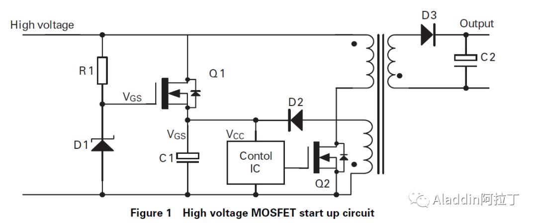
Operation
Figure 1 shows the MOSFET start up circuit where the MOSFET is biased on by a low current in R1 to form a resistive pass element. C1 charges up to the point where the control IC becomes active, the maximum value of VCC in this phase are limited by Zener voltage D1 minus VGS.
Once the control IC becomes active drive pulses are issued to Q2 to form normal switching action in the transformer and power is now fed to the control IC via D2. It is therefore important for the designer to chose a value for D1 so that the supply via D2 is high is greater than D1 minus VGS thus biasing off Q1 in normal operation.
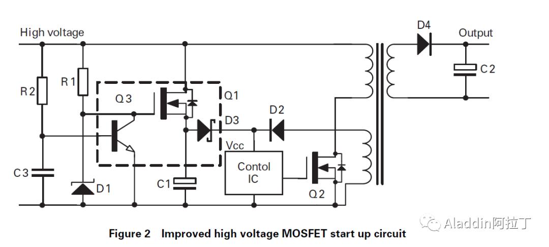
In addition to the basic requirements fault protection may be added such that if the control IC supply can not be raised by the start up circuit a time out occurs to prevent excessive dissipation in the start up MOSFET. By using an additional transistor a simple circuit could be constructed as shown in Figure 2.
Figure 2 shows the modified circuit with a time out function to prevent Q1 remaining on and over heating if the power supply can not start. Q3 is simply turned on after a delay from the time constant of R2 and C3. This circuit provides additional protection under all operating conditions and allows the use of smaller devices than if constant on time of Q1 in a fault mode had to be designed for.
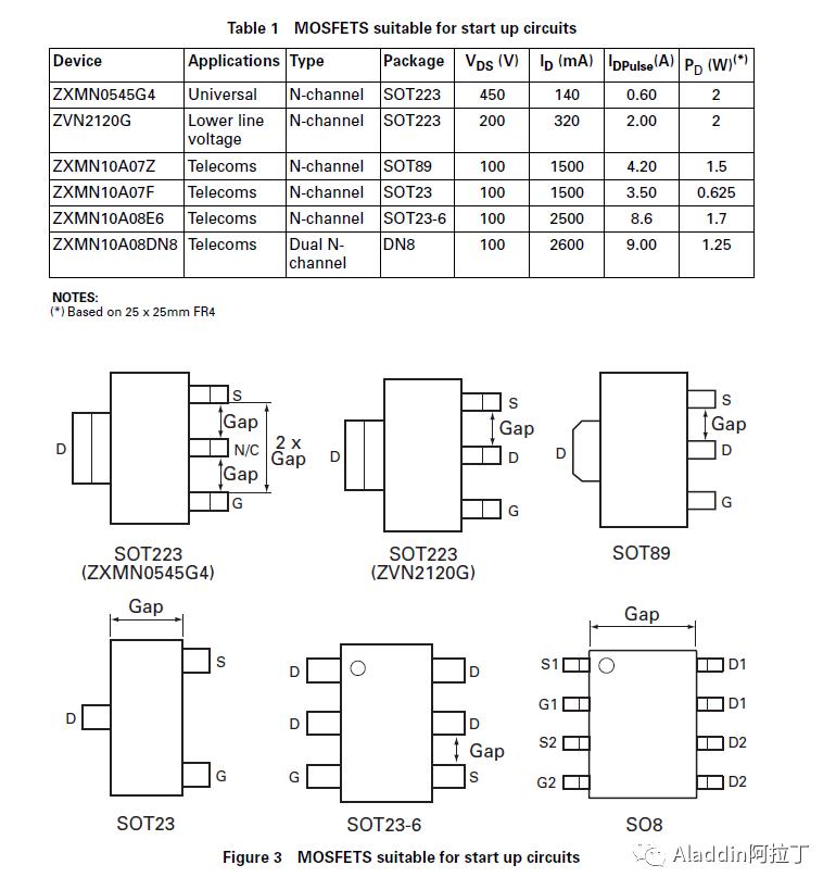
Zetex manufactures a range of medium voltage MOSFETS and bipolar transistors suitable for use in this application contained in small outline packages with some offering additional pin spacing for creepage distance compliancy.
The use of Zetex medium voltage bipolar transistors in switch mode power supplies
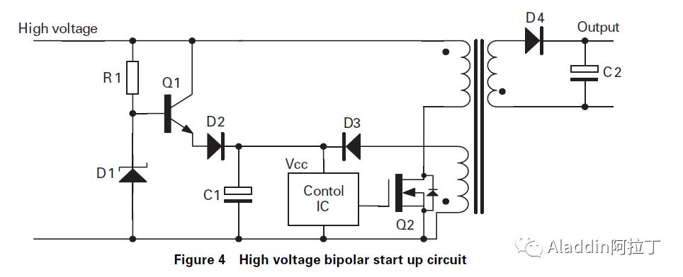
Operation
Figure 4 shows the Zetex bipolar start up circuit where the bipolar Q1 is biased on by a low current in R1 to form a resistive pass element. C1 charges up to the point where the control IC becomes active. The maximum value of VCC in this phase is limited by Zener voltage D1 minus VBE of Q1 and the VF of D2.
Once the control IC becomes active drive pulses are issued to Q2 to form normal switching action in the transformer and power is now fed to the control IC via D3. It is therefore important for the designer to chose a value for D1 so that the supply via D2 is high is greater than D1 minus VBE Q1 thus biasing off Q1 in normal operation.
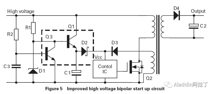
In addition to the basic requirements fault protection may be added such that if the control IC supply can not be raised by the start up circuit a time out occurs to prevent excessive dissipation in the start up bipolar. By using a small outline Zetex transistor a simple circuit could be constructed as shown in Figure 5.
Figure 5 shows the same circuits with a time out function to prevent Q1 remaining on and over heating if the power supply can not start. Q3 is simply turned on after a delay from the time constant of R2 and C3. This circuit provides additional protection under all operating conditions and allows the use of smaller devices than if constant on time of Q1 had to be designed for.
Zetex manufactures a range of medium voltage bipolar transistors suitable for use in this application contained in small outline packages.

2. MicrochipпјҢдё“з”ЁеҗҜеҠЁеҷЁд»¶LND150NпјҢSupertexиў«Microchip收иҙӯ
Efficient Switch mode Power Supply Start-Up Circuit
Reference Design using part LND150N3 by Microchip Technology

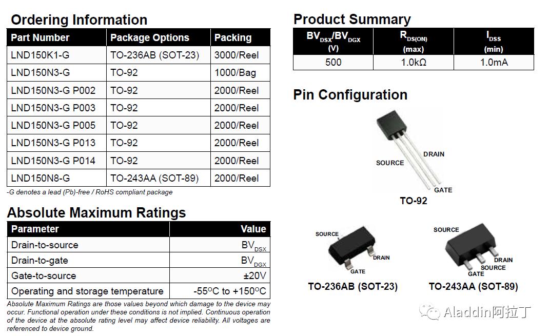
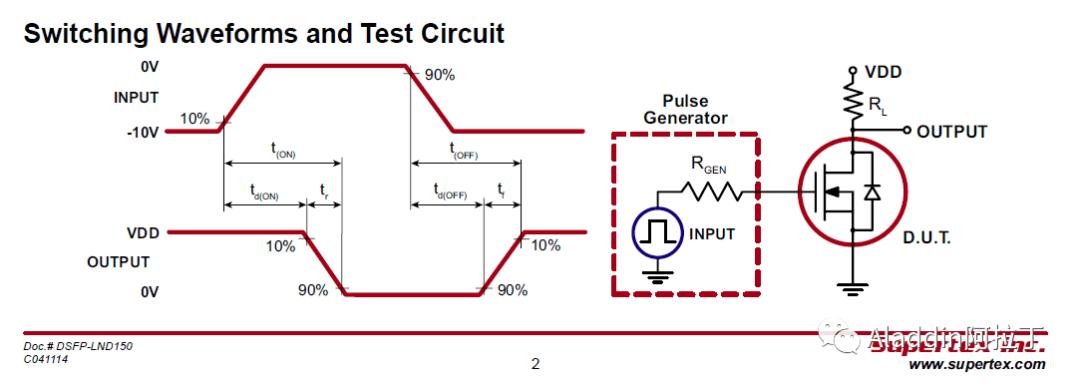
Efficient Switch mode Power Supply Start-Up Circuit. The purpose of this application note is to many advantages of using the Supertex LND150N3 in the start-up circuit for switch mode power supplies. Commonly used low voltage bipolar, CMOS and BiCMOS switch mode power supply PWM ICs usually operate from supply voltages of up to 18V.

3. TIе®ҪеҺӢй«ҳеҺӢз”өжәҗдёӯзҡ„еҝ«йҖҹеҗҜеҠЁ
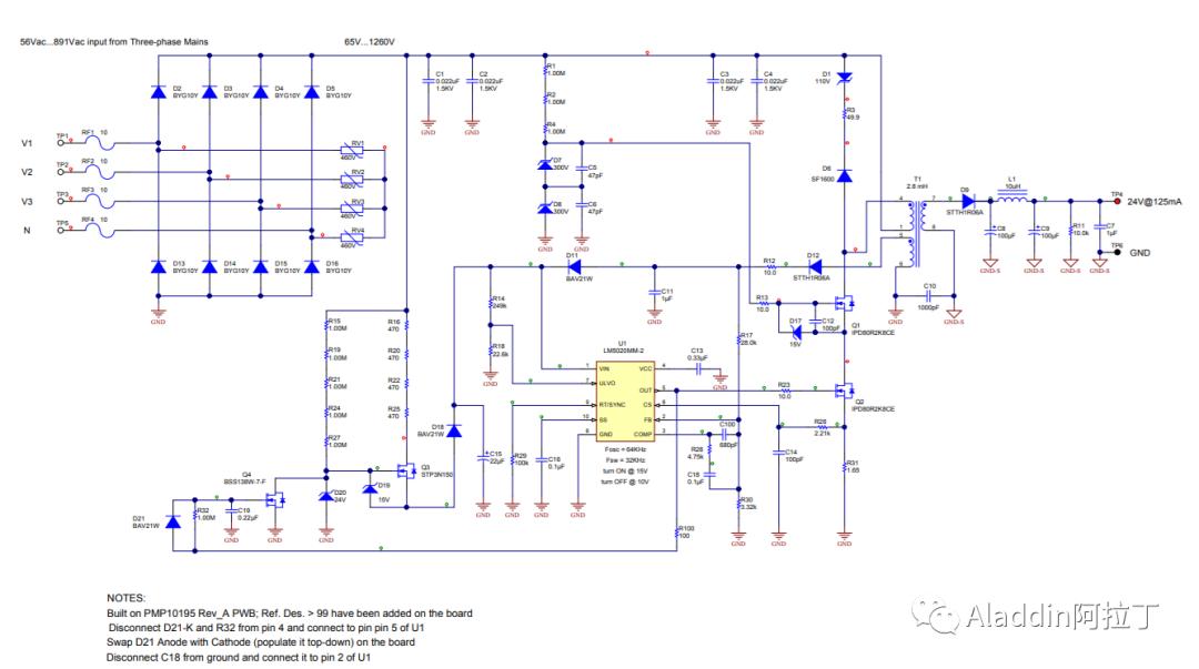
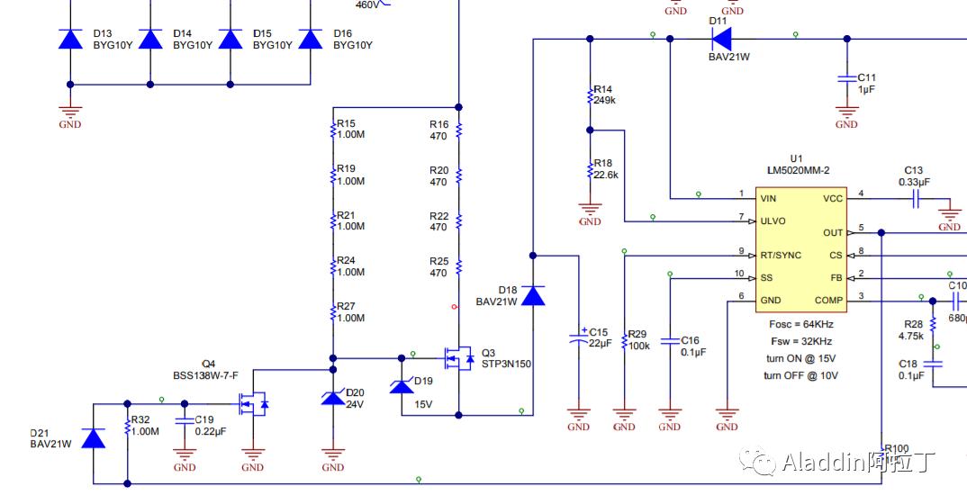
ејҖе§ӢHVжҜҚзәҝеҜ№R15-R27е……з”өпјҢеҜјйҖҡQ3пјҢHVйҖҡиҝҮR16-R25-Q3-D18/C15ж”Ҝи·Ҝеҝ«йҖҹе……з”өиҫҫеҲ°VINпјҢU1 ICжңүй©ұеҠЁиҫ“еҮәж—¶пјҢйҖҡиҝҮй«ҳз”өеҺӢеҜјйҖҡQ4, Q4жӢүдҪҺпјҢQ3ж–ӯејҖпјҢVCCз”ұиҫ…еҠ©з»•з»„жҺҘз®ЎгҖӮдҪҶR15-R27ж”Ҝи·ҜдёҖзӣҙжҚҹиҖ—гҖӮ
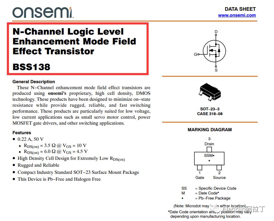
BSS138: 常规еўһејәеһӢMOSFETпјҢйҖ»иҫ‘еһӢMOSFET
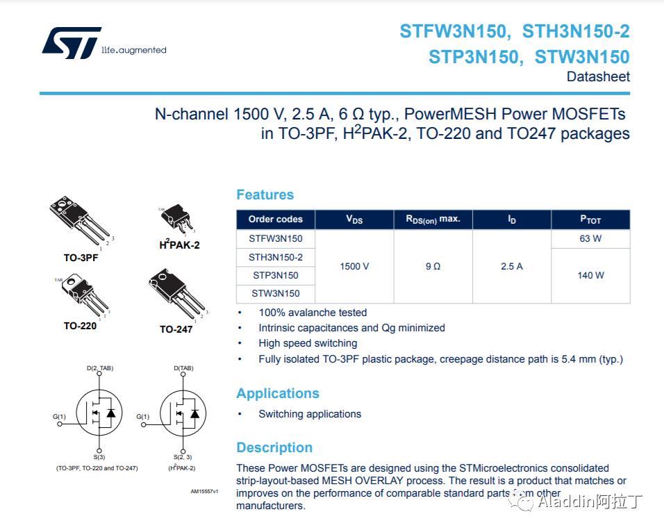
STP3N150пјҡ1500V еҠҹзҺҮеўһејәNжІҹйҖҡMOSFET
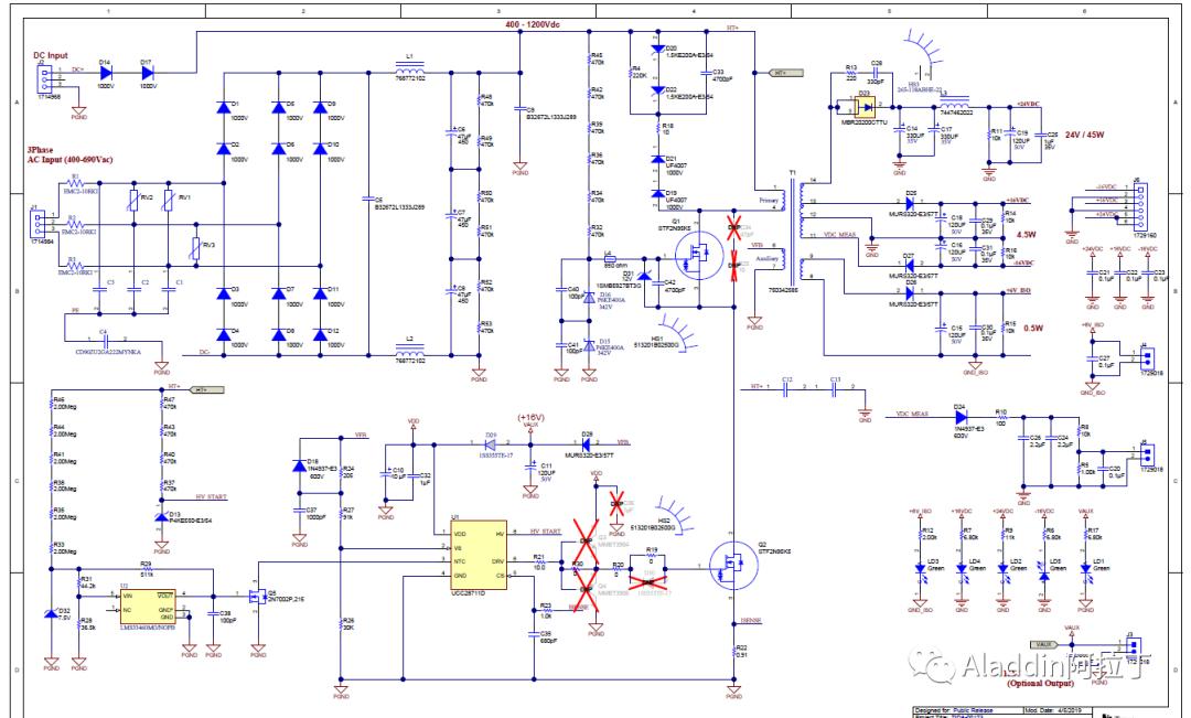
4. TIе®ҪеҺӢй«ҳеҺӢз”өжәҗдёӯзҡ„еҝ«йҖҹеҗҜеҠЁ-2
TIDA-00173пјҢ400-V to 690-V AC Input, 50-W Flyback Isolated Power Supply Reference Design for Motor Drives
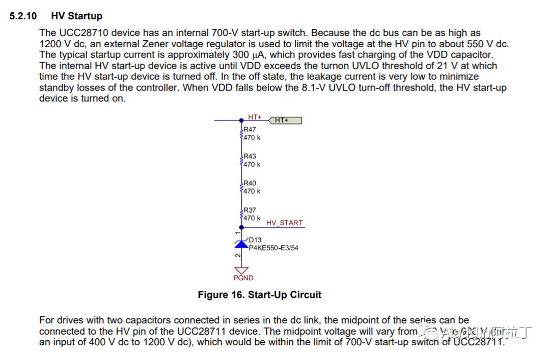
5. зҪ—е·Ҙзҡ„ж–°з”өе…ғзҡ„дәӨй”ҷPFC+LLCж–№жЎҲдёӯз”ЁеҲ°зҡ„пјҢиҝҷд№ҹжҳҜжңҖ常规зҡ„еҠ йҖҹеҗҜеҠЁз”өи·Ҝж–№жі•
https://www.dianyuan.com/bbs/2510816.html
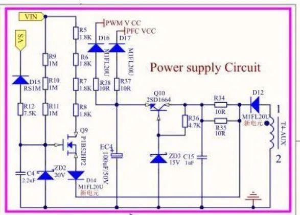
е…¶дёӯVSдёәеҚҠжЎҘз”өеҺӢдёӯзӮ№гҖӮ
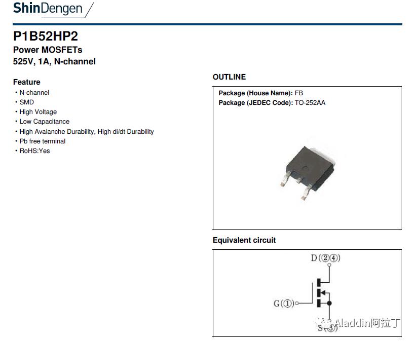
Q9дёәпјҡP1B52HP2пјҡ
6. TI UCC25600: How to design aux supply for fast startup
https://e2e.ti.com/support/power-management-group/power-management/f/power-management-forum/784870/ucc25600-how-to-design-aux-supply-for-fast-startup
7. ST-AN5335
35W transition-mode flyback converter with ultra-low THD based on HVLED007
https://www.st.com/resource/en/application_note/an5335-35w-transitionmode-flyback-converter-with-ultralow-thd-based-on-hvled007---stmicroelectronics.pdf
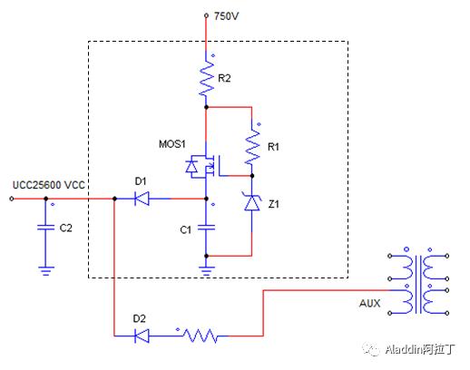
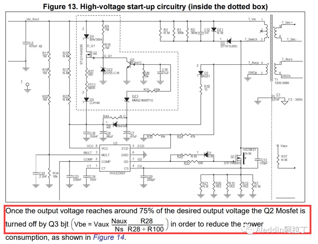
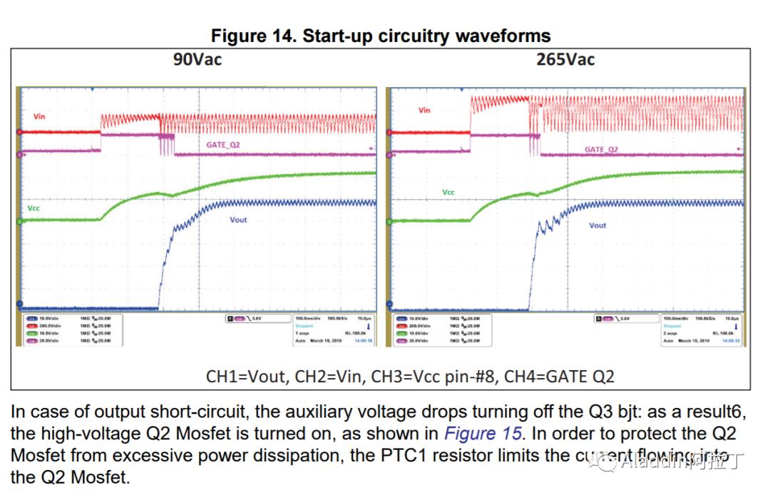
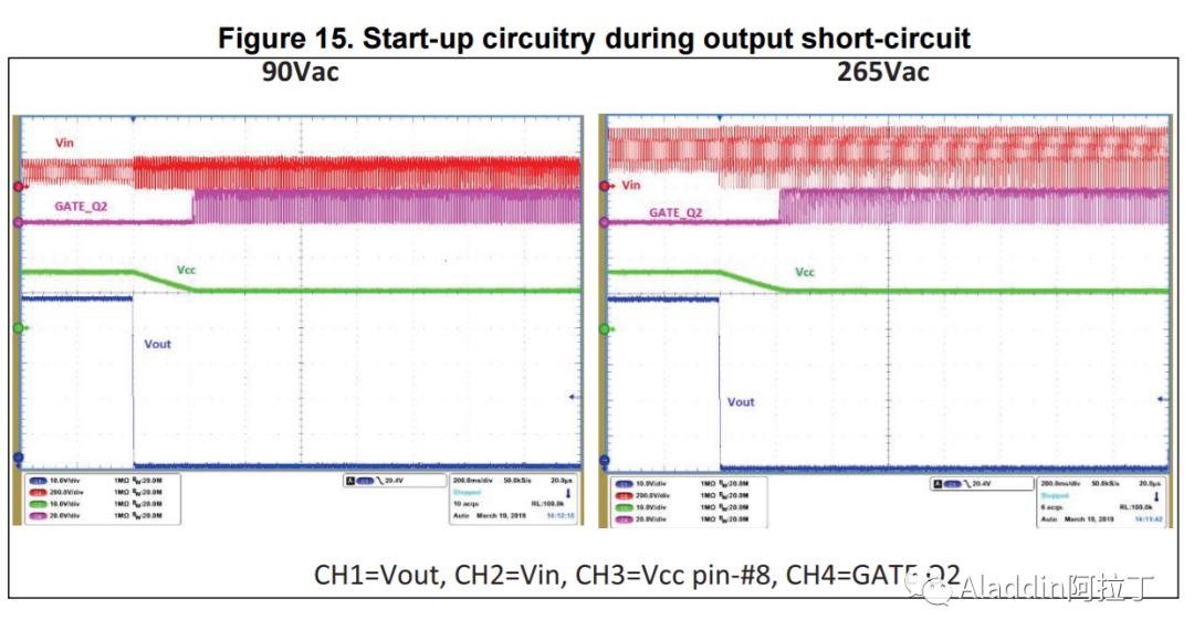
To achieve a fast startup, typically required in lighting applications, a high-voltage start-up circuitry (which is mainly composed by the high-voltage Mosfet Q2), charges the VCC pin voltage. Once the VCC pin voltage reaches the IC turn-on threshold (12.5 V typ.), the HVLED007 starts the operations. The high-voltage start-up circuitry is then turned off, to limit the power dissipation, once the output voltage reaches around 75% of the target.
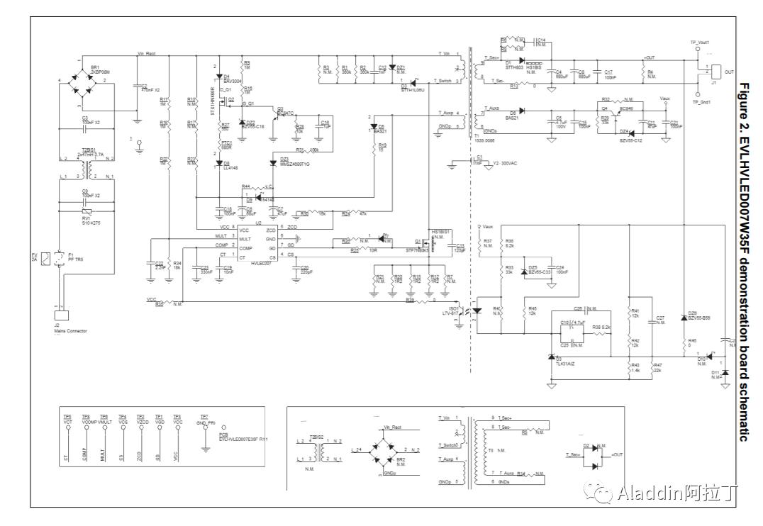

й«ҳеҺӢеҝ«йҖҹеҗҜеҠЁз”өи·Ҝз»ҶиҠӮ
Figure 13. High-voltage start-up circuitry (inside the dotted box)
8. IWATT/Dialogиө„ж–ҷпјҢйҮҮз”ЁиҖ—е°ҪеһӢMOSдҪңдёәеҗҜеҠЁз”өи·Ҝ
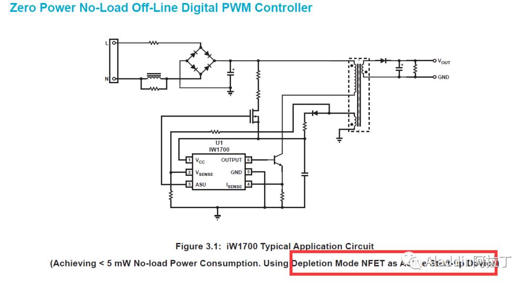
жҲ–NPN BJT

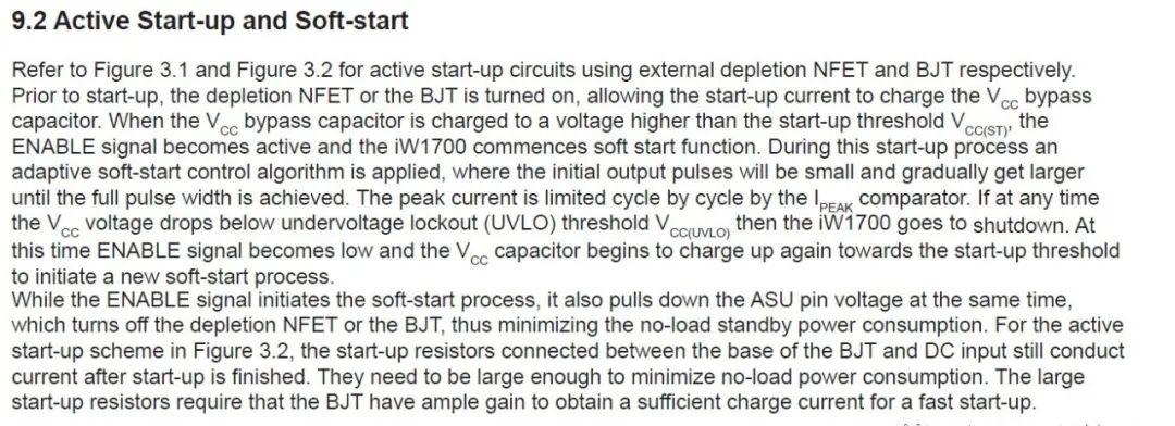
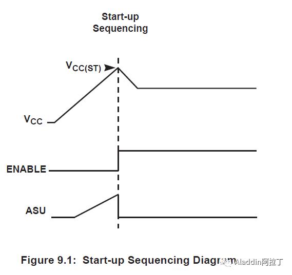
е®ғ们家зҡ„ICжҜ”иҫғзү№ж®ҠпјҢеҚ•зӢ¬жңүдёҖдёӘеј•и„ҡдҪңдёәеҗҜеҠЁж”Ҝи·Ҝе…іж–ӯпјҢ иҝҷж ·дёҚйңҖиҰҒд»Һе…¶д»–ең°ж–№еҶҚеј•дҝЎеҸ·жқҘе…іж–ӯиҝҷдёӘж”Ҝи·ҜгҖӮ
9. TI, SLUA752вҖ“August 2015
Isolated 70-W Streetlight LED Driver Using UCC28810
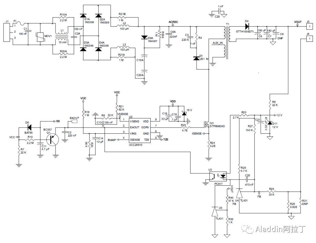
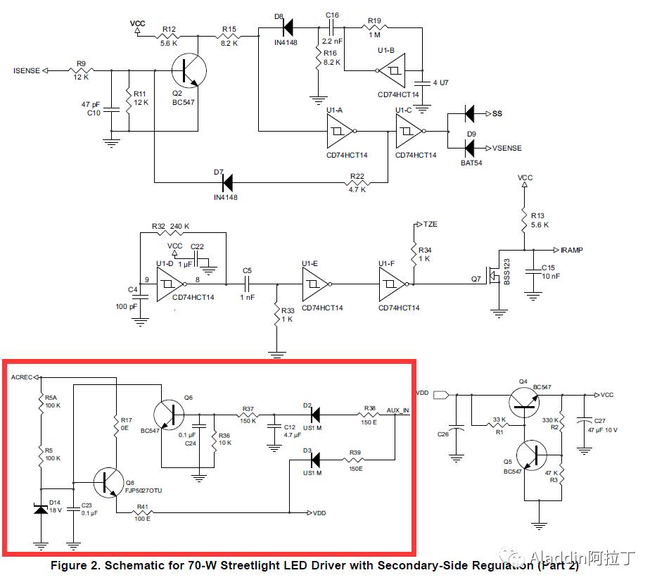
It is not possible to supply bias voltage while meeting IC current requirements for both UCC28810 and CD74HCT14 together using the resistive startup technique. In Figure 5, transistor Q8 as emitter-follower sources 17.4 V VDD startup bias for UCC28810 at its emitter, which is converted to 5 V for CD74HCT14 supply using discrete, low-IQ linear regulator. Once switching begins and output voltage ramps-up, bias voltage for these ICs is sourced from primary-side auxiliary winding, which is also used to disable activestartup circuit with Q6. Once in steady state, it is required to disable active-startup circuit in order to minimize efficiency loss due to large voltage drop across Q8 and IC supply current flowing through it.

10. TI-EDN-Keeping it green with faster startup and less standby power
涓жөҒе……з”өпјҢиҮӘдёҫеҗҜеҠЁз”өи·Ҝ
https://www.edn.com/keeping-it-green-with-faster-startup-and-less-standby-power/
To help reduce standby power, in this article I will discuss startup circuitry that replaces traditional bootstrap startup circuitry, which only dissipates power during power up. This environmentally green circuitry has the added benefit of providing much faster startup when compared to traditional bootstrap circuitry.
Let us review the traditional bootstrapping circuitry of an offline adapter (Figure 1). The bootstrapping is formed by a trickle-charge resistor (RT) and a holdup capacitor (CDD). This circuitry is very inexpensive and has worked quite well over the years. It has two issues that are worth discussing.
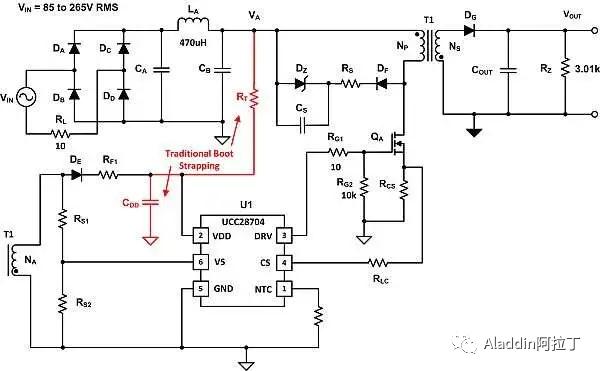
The trickle charge resistor RT вҖҳs main purpose is to provide a current path for charging U1вҖҷs bias and holdup capacitor (CDD). The CDD capacitor will supply energy temporally to U1 during power, until the auxiliary winding (NA ) has enough energy to power the controller. The issue with this technique is that after bootstrapping is complete, the resistor, RT, is not needed and will continue to dissipate power (PRT ) unnecessarily. The power dissipated by RT could make it difficult to pass the DoE 100 mW standby power requirement. For example, if a 1-MО© resistor used for bootstrapping would dissipate roughly 26 mW (Equation1), this is roughly 26% of the DoEвҖҷs standby power requirement.

Control integrated circuit (IC) manufacturers have reduced the standby current of their power-supply controllers, so you can use an RT of 15.33 MО© or more for these bootstrapping circuits. This will cut idle power losses down by a factor of 15 or more; however, it will also increase the amount of time it takes to start up the power supply. For example, with a power-supply controller bypass capacitor (CDD) of 330 nF, a power-supply controller turn-on voltage (VVDD(on) ) of 21 V, a minimum input voltage of 85-V root mean square (RMS) and an IC startup current (ISTART) of 2.5 ВөA, it could take up to 1.3 seconds (tON) just for the power converterвҖҷs controller to become active.

The circuitry presented in Figure 2 speeds up startup time and reduces standby power. The circuitry highlighted will replace RT ; this circuitry is formed by a depletion-mode MOSFET (Q1) that an NPN transistor (Q2) will turn on and off. This switch will be controlled by the voltage provided by an external reference (VB) from the pulse-width modulation (PWM) controller, which activates once the PWM controller becomes active.
In the circuit example provided in Figure 2 , this control function comes from the NTC pin of the PWM controller. Resistor RL protects Q1 and U1 from an overcurrent condition and overvoltage. Resistors R1 and R2 form a high-impedance voltage divider that when pulled low will turn off FET Q1. Resistor R3 limits the current into the base of transistor Q2. By adding capacitor C1, the control voltage does not have to be a steady-state DC voltage вҖ“ it can be a PWM signal as well вҖ“ and could even be driven by the PWMвҖҷs gate driver. Capacitor C1 and Resistors R1 and R2 form a turn-off delay when using a PWM signal.
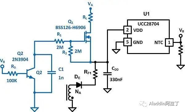
Some primary-side regulator (PSR) controllers initiate a device shutdown and restart when a system fault occurs by discharging CDD with a fixed discharge current (IFAULT). It is important to size RL to limit the maximum charge current to roughly half of this fault pull-down current (IFAULT) maximum. In this design example, the IFAULT of the controller is 2 mA and RL would be roughly 375 kО©. Please note that this will slow down the startup at low line; however, will be greatly improved over the trickle-charge bootstrap startup circuitry.

To show how much faster this startup circuit is, let us review the longest startup time required to turn on the power-supply controller (U1) using the fast startup and compare it to traditional startup circuitry. Please note that this circuit will take roughly one-fourth of an input line cycle to become active. The controller will take the longest time to start up (tON) at the minimum input voltage (85-V RMS) and a 60-Hz line frequency (fLINE). The estimated startup time would be roughly about 26 ms, roughly 50 times faster than the trickle-charge startup circuity discussed earlier---еҗҜеҠЁйҖҹеәҰеҝ«50еҖҚ.

To evaluate this fast startup circuit even further, I evaluated a 10-W USB adapter using the Texas Instruments UCC28704 PSR controller. This converter used a trickle-charge bootstrapping scheme. RL was 15.33 MО©: three 5.11-MО© resistors in series. The controls IC bypass capacitor (CDD ) used for bootstrapping was 330 nF. Then, I powered up the converter under a minimum input of 85-V RMS and input voltage (VIN ) and evaluated the control ICs, VDD, NTC and gate-driver (DRV) pins. When I powered up the adapter under full load, it took roughly 1.3 seconds for the power-supply controller to become active. You can see this in Figure 3 вҖҷs oscilloscope plot, which shows the difference VIN was applied and when the UCC28704вҖҷs gate driver (DRV) becomes active and starts switching. The power-supply startup time was also close to the earlier mathematical estimate in this article.

Figure 3 Trickle charge startup, tON вүҲ 1.3 s 涓жөҒе……з”өеҗҜеҠЁж—¶й—ҙ:1.3з§’
Next, I removed RT and added the fast startup circuit shown in Figure 4 to the adapter. I then tested the adapter under the same test conditions and monitored the same nodes discussed above. When applying the minimum input voltage of 85-V RMS, it took roughly 27 ms for the power-supply controllerвҖҷs gate drive to become active. This startup time was roughly 48 times faster than using the trickle-charge bootstrapping scheme. This startup time was roughly 4 percent higher than the mathematical estimation. Under no load (at 265-V RMS), this adapter dissipated less than 55 mW of output power, easily meeting the DoE and European Code of Conduct (CoC) input standby power requirements.

Figure 4 Fast startup circuit, tON вүҲ 27 ms
To help reduce cost in your power-supply designs, speed up transient response and reduce input standby power, some power-supply controller manufacturers have put this fast, intelligent, green startup circuitry into their flyback controllers, including the Texas Instruments UCC28730. However, if your design is using a flyback controller that uses a trickle-charge bootstrapping scheme and you canвҖҷt get a fast enough startup time to meet the standby power requirements that your design requires, you can use the circuitry presented in this article to speed up your designвҖҷs startup time as well as reduce standby power.
11. MircochipпјҢBOOTSTRAP DESIGN иҮӘдёҫдҫӣз”өи®ҫи®Ў
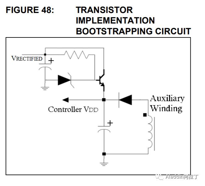
In some power-supply applications, the Pulse-Width Modulator (PWM) controller is powered from an auxiliary winding, tapped off the power stageвҖҷs transformer. This technique is used to reduce power loss. The only drawback is at start-up as the capacitor needs to be trickle charged from the rectified voltage, as shown in Figure 47. Another discrete technique to start-up the circuit is depicted in Figure 48.
These techniques work well but they have the following disadvantages:
вҖў Inefficiency вҖ“ Draws current continuously from the high-voltage source
вҖў Poor dynamic range вҖ“ bias must be set for the minimum input voltage (at high-input voltage, the current drawn is higher)
вҖў Poor regulation
вҖў No current limit
вҖў No overtemperature protection
вҖў Requires large power resistor and Zener diode

12. жқӮйЎ№
https://www.industrial-electronics.com/switching-power-supply_1-8.html
DISSIPATIVE (PASSIVE) START CIRCUITж— жәҗжҚҹиҖ—еҗҜеҠЁз”өи·Ҝ

Resistive, dissipative start circuit, providing initial low-voltage auxiliary power needs from the 300-V DC supply.
A regulating zener diode ZD1 prevents excessive voltage being developed on C3. The charge on C3 provides the initial auxiliary power to the control and drive circuits when converter action is first established. This normally occurs after the soft-start procedure is completed.
The auxiliary supply is supplemented from a winding on the main transformer T1 when the converter is operating, preventing any further discharge of C3 and maintaining the auxiliary supply voltage constant.
A major requirement for this approach is that sufficient start-up delay must be pro vided in the main converter to permit C3 to fully charge. Further, C3 must be large enough to store sufficient energy to provide all the drive needs for correct start-up of the converter.
In this circuit, R1 and R2 remain in the circuit at all times. To avoid excessive dissipation the resistance must be high, and hence the standby current requirements of the drive circuit must be low prior to converter start-up. Since C3 may be quite large, a delay of two or three hundred milliseconds can occur before C3 is fully charged. To ensure a good switching action for the first cycle of operation, C3 must be fully charged before start-up, and this requires a low-voltage inhibit and delay on the start-up control and drive circuits.
To its advantage, the technique is very low cost, and resistors R1 and R2 can perform dual duty as the normal safety discharge resistors that are inevitably required across the large storage capacitors C1 and C2.
TRANSISTOR (ACTIVE) START CIRCUIT BJTжңүжәҗеҗҜеҠЁз”өи·Ҝ
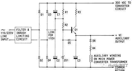
The basic circuit of a more powerful and fast-acting start system, incorporating a high-voltage transistor Q1.
Lower-dissipation, active transistor start circuit, providing initial low-voltage auxiliary supply needs from the 300-V DC supply.
In this arrangement, the resistance of R1 and R2 and the gain of Q1 are chosen such that transistor Q1 will be biased into a fully saturated "on" state soon after initial switch-on of the supply.
As C1 and C2 charge, current flows in R1 and R2 to the base of Q1, turning Q1 fully on. Zener diode ZD1 will not be conducting initially, as the voltage on C3 and the base of Q1 will be low. With Q1 turned on, a much larger current can flow in the low-resistance R3 to charge C3.
In this circuit, resistor R3 can have a much lower value than R1 and R2 in the circuit shown in FIG. 8.1. This will not result in excessive dissipation or degrade the efficiency, as current will flow in R3 only during the start-up period. Transistor Q1 will turn off after C3 has charged and will be operating in the cut-off state after the start-up period; hence its dissipation will also be very low. R3 should be chosen to have a high surge rating (i.e., it should be wirewound or carbon composition).
After switch-on, capacitor C3 will charge up relatively quickly, raising the voltage on Q1 emitter, and the base will track this rising voltage +Vbe until it arrives at the zener volt age ZD1. At this point ZD1 starts to conduct, forcing Q1 into linear operation and reducing the charge current into C3. The voltage and dissipation will now build up across Q1.
However, once converter action is established, regenerative feedback from the auxiliary winding on the main transformer will provide current via D6 and resistor R4 to capacitor C3. Hence the voltage on C3 will continue to increase until the base-emitter of Q1 is reversed-biased and it is fully turned off.
At this point, diode D5 is brought into conduction, and the voltage across C3 will now be clamped by the zener diode ZD1 and diode D5. The dissipation in ZD1 depends on the values of R4 and the maximum auxiliary current. With Q1 off, the current in R3 ceases, and its dissipation and that of Q1 will fall to zero.
As the start-up action is fast, much smaller components can be used for R3 and Q1 than would otherwise be necessary, and heat sinks will not be required. To prevent hazardous dissipation conditions in Q1 and R3 in the event of failure of the converter, the circuit should be "fail safe" and should be able to support continuous conduction. Fusible resistors or PTC thermistors, with their inherent self-protection qualities, are ideal for this application.
This circuit is able to supply considerably more start-up current and gives greater freedom in the design of the drive circuit.
IMPULSE START CIRCUITSи„үеҶІеҗҜеҠЁз”өи·ҜпјҢеҲ©з”ЁDIAC
дҪ•дёәDIAC:
T786-з…§жҳҺ-и°ғе…үеҷЁ-и°ғе…үжҺ§еҲ¶еҷЁд»¶-Triode/TRIAC/SCR... жқҘжәҗпјҡзҪ‘з»ң
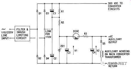
Diac impulse start circuit, providing initial low-voltage auxiliary needs from the 300-V DC supply.
a typical impulse start circuit, which operates as follows.
Resistors R1 and R2 (normally the discharge resistors for the reservoir capacitors C1 and C2) feed current into capacitor C3 after switch-on. The auxiliary supply capacitor C4 will be discharged at this time.
The voltage on C3 will increase as it charges until the firing voltage of the diac is reached. The diac will now fire and transfer part of the charge from C3 into C4, the transfer current being limited by resistor R3.
The values of capacitors C3 and C4 and the diac voltage are chosen such that the required auxiliary voltage will be developed across C4 and the converter will start via its normal soft-start action.
Once again, by regenerative feedback (via D5 and the auxiliary winding), the auxiliary power is now provided from the main transformer. As C4 is further charged and its voltage increases, the diac will turn off since the voltage across it can no longer reach the firing value (because of the clamping action of ZD1 on C3). This arrangement has the advantage of supplying a high current during the turn-on transient, without excessive dissipation in the feed resistors R1 and R2. In the rare event of the converter failing to start on the first impulse, the start-up action will repeat as soon as capacitor C4 has discharged and C3 recharged to the appropriate firing value for the diac.
The choice of diac is important. It must be able to deliver the required turn-on current, and its firing voltage must be less than V1-Vstart and greater than V1-V2; otherwise lockout can occur after the first impulse. It is possible to replace the diac with a small SCR and an appropriate gate drive circuit.
е…¶д»–зӣёе…іеҝ«йҖҹеҗҜеҠЁзҡ„з”өи·ҜеҶ…е®№пјҡ
==е®Ң==
жң¬е…¬дј—еҸ·е…¶д»–жүҖжңүдё“иҫ‘жұҮжҖ»пјҡ
| | | | | | | | | | | | | | | |
е…¶дёӯ зүҮиҜӯжқӮи°Ҳ дё»иҰҒжҳҜз”ЁжқҘи®°еҪ•иҮӘе·ұзҡ„дёҖдәӣйҡҸж„ҹд№Ӣзұ»...
===================================
е…ідәҺжң¬дәәпјҡ
Eric Wen (ж–ҮеӨ©зҘҘ)
IEEE Senior Member, й«ҳзә§е·ҘзЁӢеёҲиҒҢз§°пјҲеүҜй«ҳзә§пјүпјҢдёӯеӣҪз”өеӯҗеӯҰдјҡзү©иҒ”зҪ‘йқ’е№ҙдё“дёҡжҠҖжңҜз»„йҖҡдҝЎе§”е‘ҳ(AIoT),дёӯеӣҪз…§жҳҺеӯҰдјҡй«ҳзә§дјҡе‘ҳпјҢдёӯеӣҪз”өжәҗеӯҰдјҡз…§жҳҺз”өжәҗдё“дёҡ委е‘ҳдјҡ委е‘ҳ,дёӯеӣҪз”өжәҗеӯҰдјҡйқ’е№ҙе·ҘдҪң委е‘ҳдјҡ委е‘ҳзӯү
дёӘдәәе…¶д»–дҝЎжҒҜеҸӮи§Ғе…¬дј—еҸ·пјҡAladdinйҳҝжӢүдёҒ
===================================
